
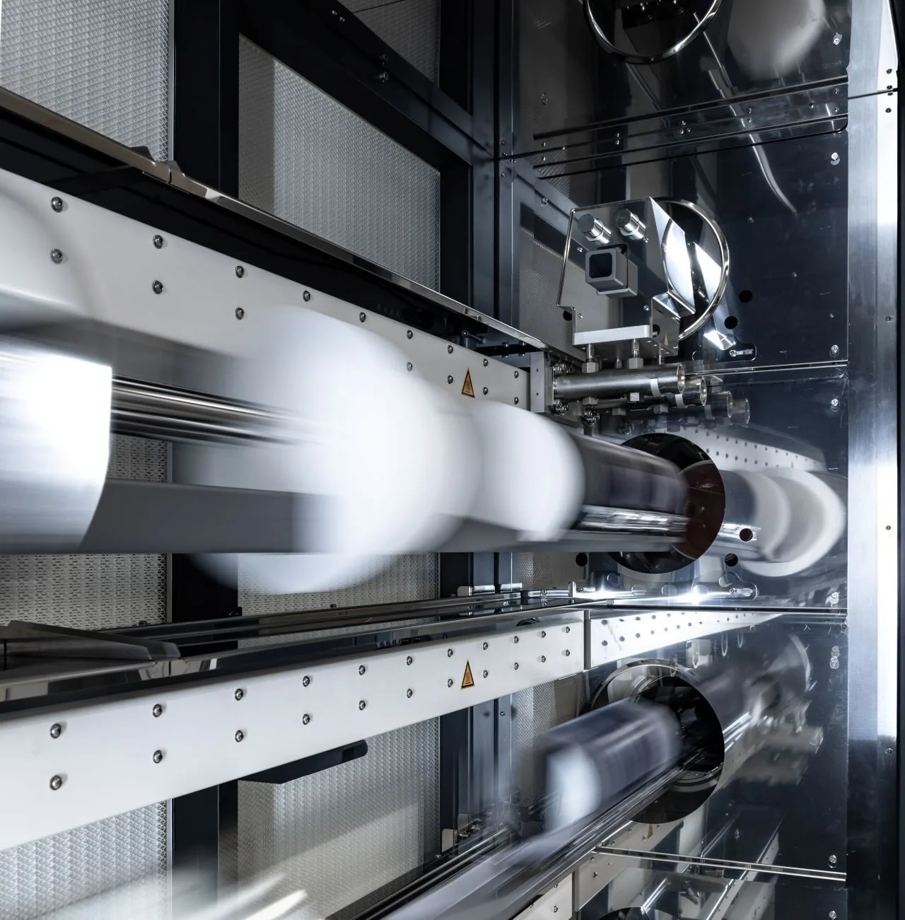
An atmospheric diffusion process is a heat treatment in a mostly inert environment which distributes dopants in a silicon, GaAs, InP or other semiconductor wafer to a desired depth, changing the electrical properties of the semiconductor. Sometimes a reactive element such as oxygen is added, consuming silicon and converting it into silicon dioxide (SiO2) for use in many applications.
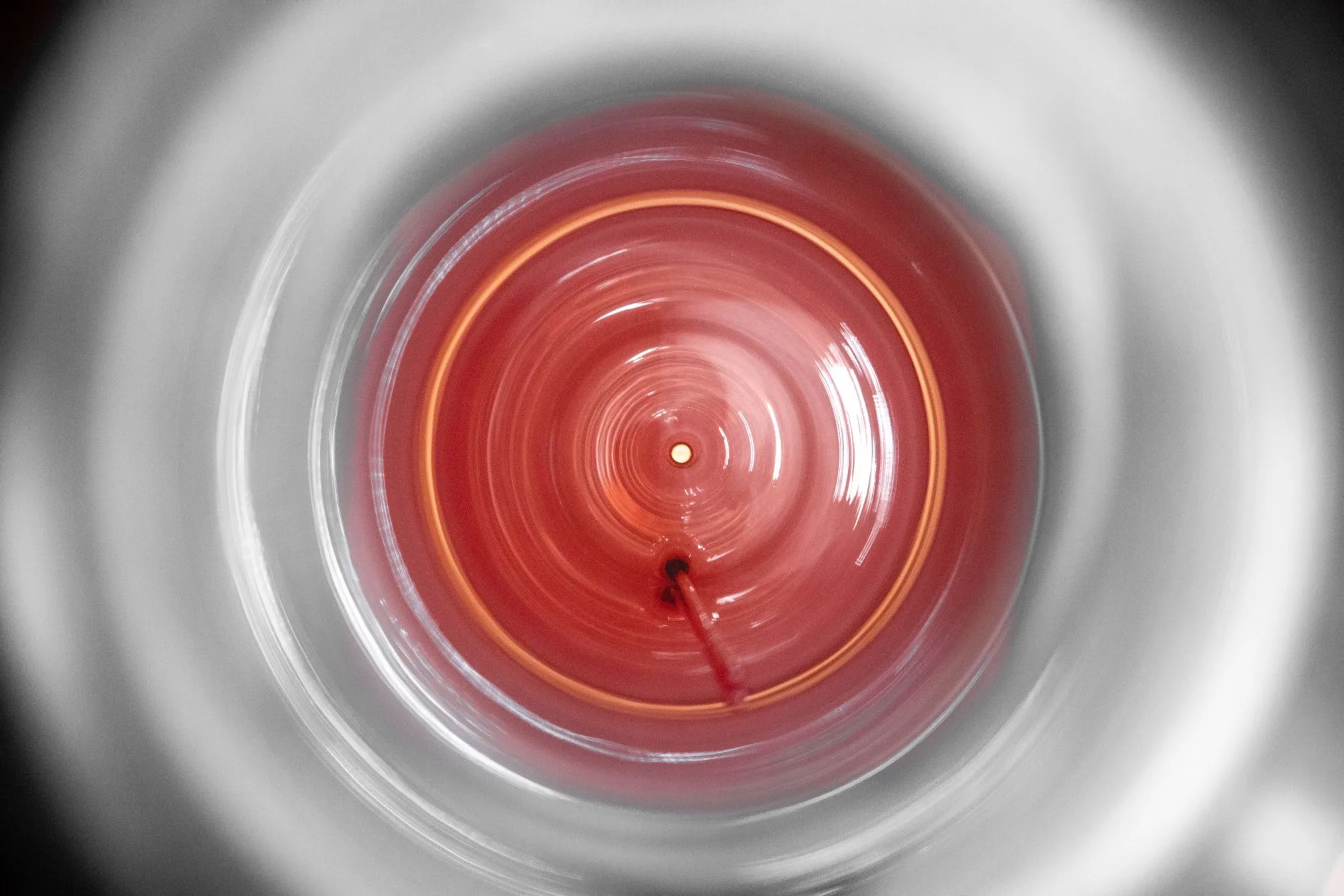
Technical principles, applications and process considerations.
An anneal is a heat treatment used to reduce stress or redistribute dopants. A metal alloy anneal reduces the electrical resistance between Si and Al contacts.
Grows layers on a wafer through a chemical reaction between oxidants and silicon atoms. The layer acts as a gate dielectric, protective coating, diffusion mask or insulating layer. The rate is limited, so dry oxidation is mainly applied to thin oxide films up to 1000 Å.
Also known as wet oxidation, used to create a thick insulating SiO2 layer. High-purity steam generated from H2 and O2 gives a much faster oxidation rate. The SiO2 layer serves as a dopant diffusion mask, junction passivation and insulating field oxide.
A wet oxidation route for extremely thick insulating SiO2 films and an economical alternative to pyrogenic oxidation. Used for diffusion masks, junction passivation, field oxide and optical insulator films of typically 8–20 µm, which may require 40 days or more of continuous processing. DI water is cheaper and safer than H2.
POCl3 creates an n-type conducting layer by first converting into a deposited P2O5 layer. The P2O5 film supplies the phosphorus dopant, which is subsequently diffused into the base material. Used in solar cell production and to generate resistors.
Dichloroethylene and trans-1,2-dichloroethylene are liquid sources for in-situ generation of ultra-high-purity HCl, used in tube cleaning and improved oxidations. The HCl removes mobile ions and transition metals from the furnace environment and wafer surface, giving oxides with lower defect densities, lower mobile ion concentrations and significantly improved minority carrier lifetime.
Low Pressure Chemical Vapor Deposition uses a chemical reaction to convert gas phase precursors into useful films. The products of that reaction are deposited on top of the wafer and therefore do not consume atoms from the base material.
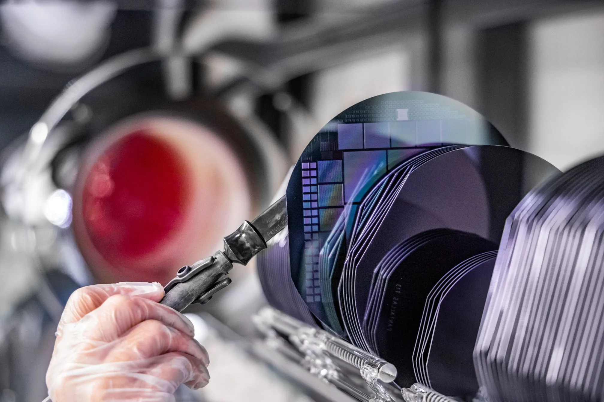
Technical principles, applications and process considerations.
Polysilicon is used as self-aligned gate electrodes and as masking material. Resistors and electrodes can be fabricated with the appropriate amount of in-situ or ex-situ doping. 'Ramped' refers to the tilted temperature profile used to counteract the depletion caused by consumption of SiH4, DCS or Si2H6.
Used where precise grain dimensions are required. 'Flat' refers to the flat temperature profile; the depletion effect is eliminated with injectors or high gas flows. Poly as bulk material in Thin Film Transistor (TFT) applications typically requires uniform grains to improve electron mobility.
Used as an insulating or masking layer in electrical and mechanical applications thanks to its chemical stability and step coverage, and as an anti-reflective coating in optical applications. A low-stress nitride process is available for thick films above 1 µm; doping nitride with oxygen yields oxynitride films for the optical industry.
Deposits an insulating SiO2 layer where excellent step coverage is required. Its medium process temperature of around 700°C minimises redistribution of implanted dopant profiles. The BPSG-doped TEOS process deposits boron- and phosphorus-doped SiO2 films at 650–700°C for cladding and passivation layers with excellent step coverage and reflow properties.
Low Temperature Oxide is mainly used as a passivation layer over devices that already have metal contacts. The low temperature reduces the electrical and mechanical properties of the deposited SiO2 film, making it typically less suitable for electrical applications.
High Temperature Oxide is an LPCVD process operating at or around 900°C that produces deposited SiO2 films with electrical and step coverage properties resembling thermally grown oxides. The high deposition temperature makes it less suitable for wafers with sensitive diffusion profiles.
Ta2O5 can replace SiO2 and Si3N4 as gate dielectric in devices such as DRAM because of its excellent electrical properties at very thin layers. Crystallising the layer with an O2 anneal generates hard, scratch-resistant masking films. It can also be combined with silicon dioxide to form high index-contrast multilayer structures for UV laser applications.
Semi-Insulating Polycrystalline Silicon is used in power devices with high voltages and currents. The atomic oxygen concentration in the polysilicon layer should be between 15 and 35 at%; above 35% the properties of SiO2 become too strong. Accurate measurement requires special tools, or the Differential Mass / Differential Thickness Method together with additional furnace tubes and etch tools.
Tempress offers furnace solutions for various other processes such as wafer splitting (SOI/POI) and polyimide curing, and is open to customise and co-develop specific thermal processes to fit your needs.
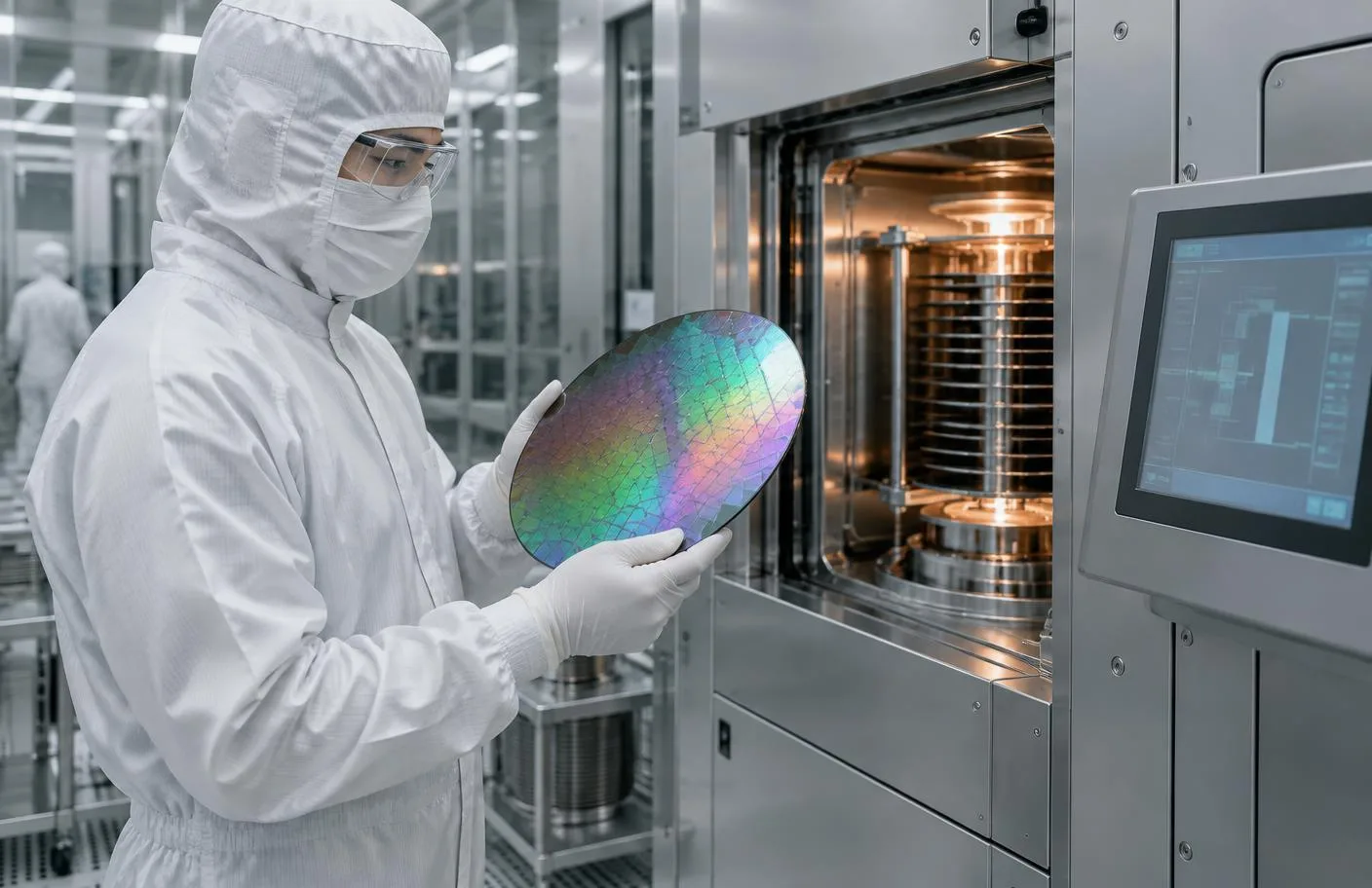
Technical principles, applications and process considerations.
Polyimides are lightweight high-performance plastics, flexible and resistant to heat and chemicals, used as mechanical stress buffers, electronic passivation layers, adhesive films in chip bonding, interlayer dielectrics and flexible cables. They are typically spin coated in liquid form, baked and thermally cured between 200 and 400°C. The bake-out removes remaining solvents and the curing anneal creates cross-linking bonds. Low oxygen values are necessary during bake-out and curing to obtain bright, uniformly coloured films with good adhesion.
Atomic Layer Deposition yields excellent step coverage and builds a film one atomic layer at a time. Unlike LPCVD or PECVD, ALD does not mix precursors but alternates them in pulses; the self-limiting surface reaction makes for a simple process set-up. For aluminium oxide, TriMethylAluminium (TMA) reacts with H2O to form Al2O3: one TMA pulse saturates the surface, excess is purged, one H2O pulse produces one atomic layer of Al2O3, and repeating the pulses gives the desired thickness — roughly 1 Å per cycle.
Atmospheric Pressure CVD for dielectric gap-fill using SiH4 or TEOS chemistry, with linear injector technology and self-cleaning heated conveyor processing for precise, repeatable and uniform gap fill. Tempress offers support, spares and upgrades for legacy WJ-999, WJ-1000 and WJ-1500 tools.
Plasma Enhanced CVD allows deposition at lower temperatures with increased deposition rates, suitable for temperature-sensitive substrates and a lower overall thermal budget than LPCVD.
Tempress ONO process combines thermal oxide growth, low-pressure nitride, and low-pressure oxide deposition without breaking vacuum, ensuring a high-quality ONO stack with repeatability and uniformity. Advanced gas distribution and temperature control systems provide consistent results across the entire wafer batch and minimize maintenance requirements.